Novel Material – Polyimide
When miniaturization of transistor is challenged by the fundamental scaling limits in recent years, advanced packaging is considered as the most promising solution for break through Moore’s law. It has the advantages of small form factor, heterogeneous integration, and reducing the RC delay. In the advanced packaging technology, polymer is commonly used as dielectric in redistribution layers (RDLs) for the applications of IC substrate, organic interposer, and fan-out packaging. In addition, hybrid bonding of polymer and metal materials has also attracted extensive attention for the fine-pitch structures. Due to the wide variety of properties required for different purposes, developing novel polymer materials and verifying their feasibility in the packaging applications has an important role in the semiconductor industry.
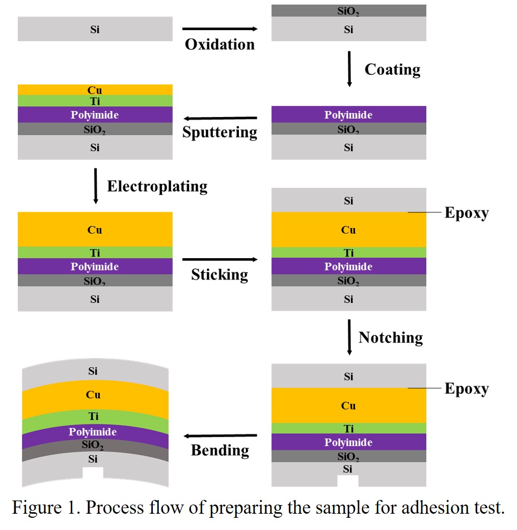
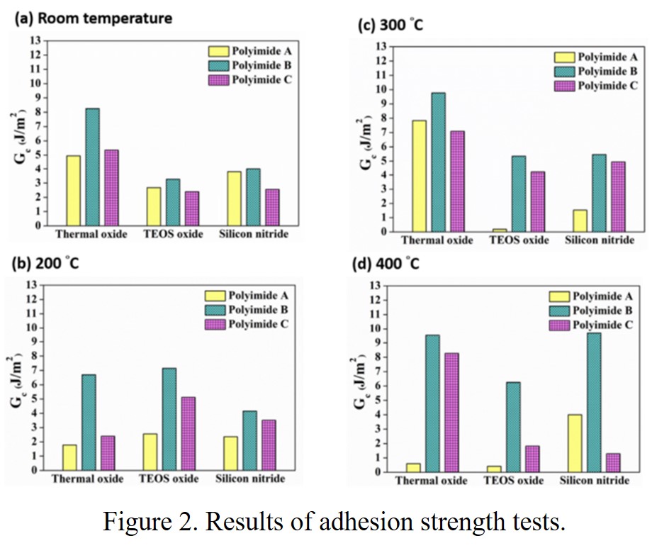
Photosensitive polyimide (PSPI) can simplify the lithography process, while the required high curing temperature leads to the difficulty in the process of polymer bonding. Therefore, it is very important to develop PSPI with the low curing temperature. Our group successfully evaluated the novel PSPI with low curing temperature by lithography test, adhesion test, and reliability test, as shown in Figure 1 and Figure 2. In addition, effects of the electroplating process on adhesion strength between Ti/Cu and polyimide materials were also discussed, further verifying the feasibility for the applications in industrial packaging structures.


