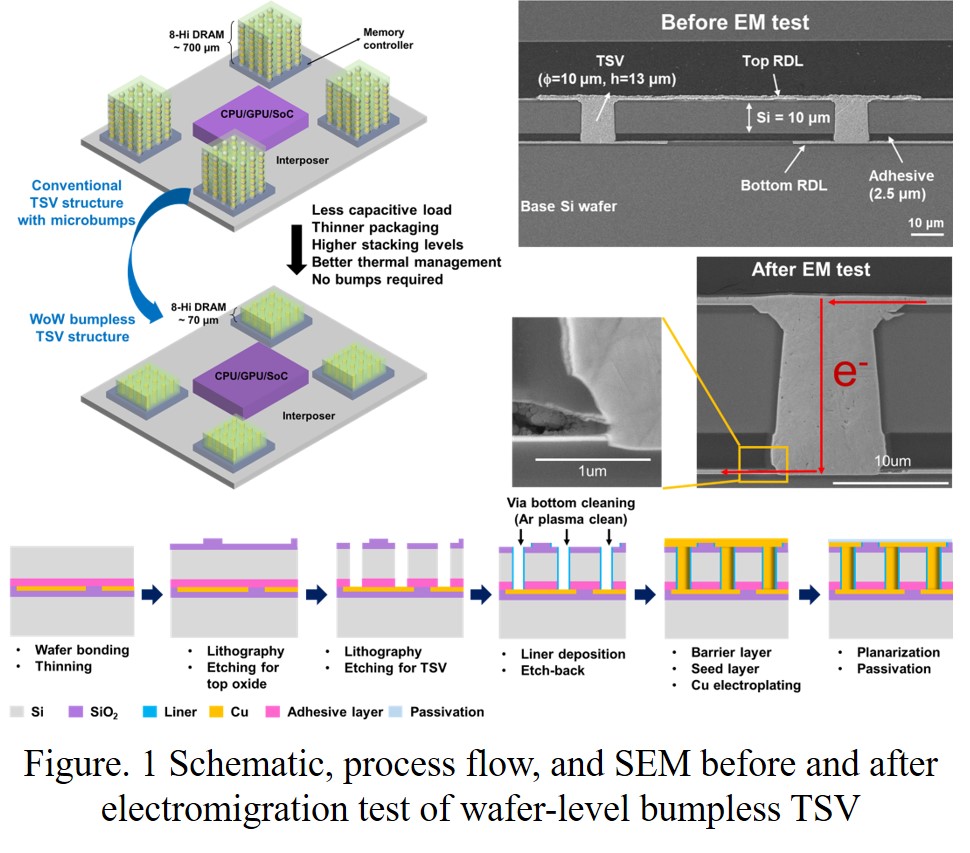
Wafer-level Bumpless Through-Silicon-Via (TSV)
For the vertically integrated architecture of 3D IC, TSV is one of the critical techniques. By utilizing vertical TSV to connect the bottom- and top-layer transistors and circuits, 3D IC possesses significantly higher efficiency of inter-chip transmission and lower power consumption than the traditional wire bonding packaging structures. However, the TSV technique suffers from issues such as the shrinkage of bump, mismatch of thermal expansion coefficient, weak anti-electromigration ability and heat conduction. Accordingly, our group proposed the wafer-level bumpless TSV technique and applied the via-bottom cleaning technique to improve the electrical performance, electromigration and reliability, as shown in Figure 1.
This wafer-level bumpless TSV technique is able to provide high throughput of packaging and feasibility for industrial application. Moreover, this bumpless structure, enabling thinner stacking, could be adaptable to the application of multi-level stacking like high bandwidth memory. We used a novel circuits model to simulate the electrical performance of the bumpless structure applying to multi-level stacking, and exhibited the via-bottom clean technique for the multi-level stacking efficiently suppressing the signal transmission loss.


