High-Precision Wafer-Level Alignment with Moiré Patterns and Deep Learning
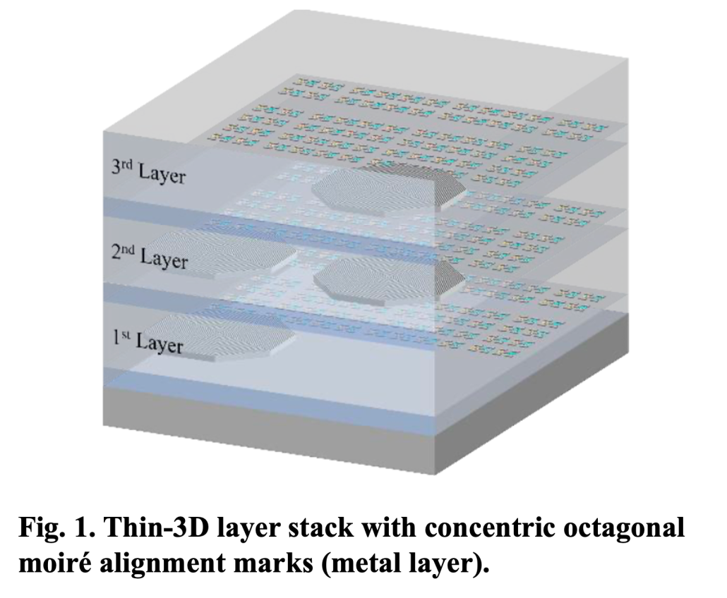
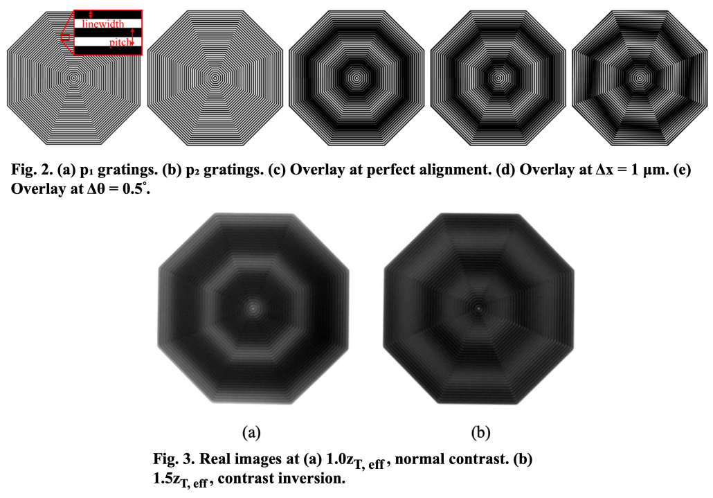
As Thin-3D ICs advance toward higher stacking density and smaller interlayer spacing, high-precision wafer-to-wafer alignment has become critical for multi-tier stacking and device integration. To address the limitations of conventional optical alignment techniques in high-precision and multi-tier applications, this work presents a high-precision wafer alignment technology combining Moiré patterns and deep learning. Concentric octagonal Moiré alignment marks are integrated into the metal layer of the chip. By utilizing the Moiré patterns generated from two periodic structures, in-plane displacement and rotational information between wafers can be converted into measurable optical signals. A single Moiré mark simultaneously provides X, Y displacement and rotational angle θ, enabling three-degree-of-freedom (3-DoF) alignment, as shown in Fig. 1. Figs. 2–3 illustrate the formation of Moiré patterns and the contrast inversion mechanism. By utilizing the Talbot effect, a working distance of approximately 90 μm is established, enabling non-contact wafer alignment.
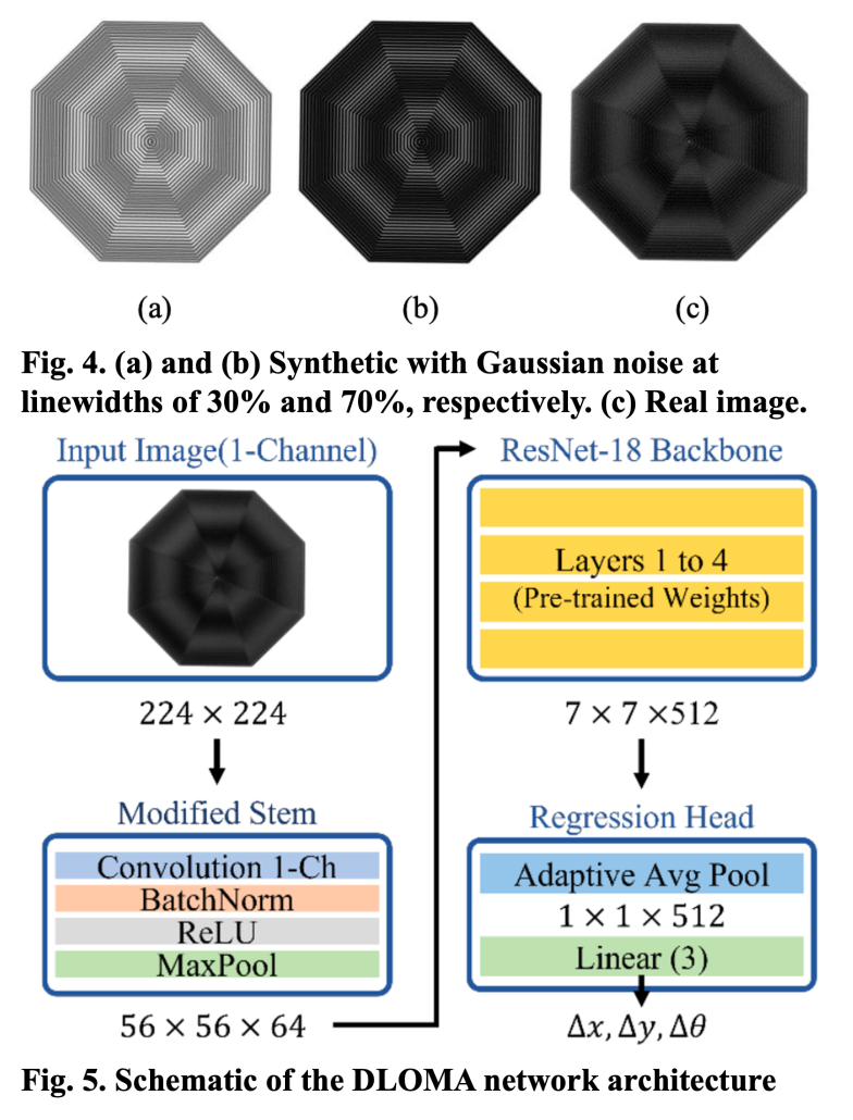
To further improve measurement accuracy and reduce the need for manual analysis, a Digital Twin framework is developed. Precisely controlled horizontal displacement and rotational angle are used as the basis for generating synthetic images, enabling the creation of a large and controllable training dataset. Image perturbations, including noise, blur, and illumination variations, are further introduced to simulate practical measurement conditions, as shown in Fig. 4.
Fig. 5 presents the Deep Learning-based Moiré Alignment (DLOMA) architecture, which integrates deep learning with Moiré patterns to directly extract X, Y, and θ information from Moiré images. Through joint training using synthetic and real images, Domain Adaptation is performed to reduce the differences in image features between simulated and experimental data. With this approach, displacement and rotational information can be directly extracted from actual wafer alignment images acquired by the alignment system, improving measurement efficiency and automation.
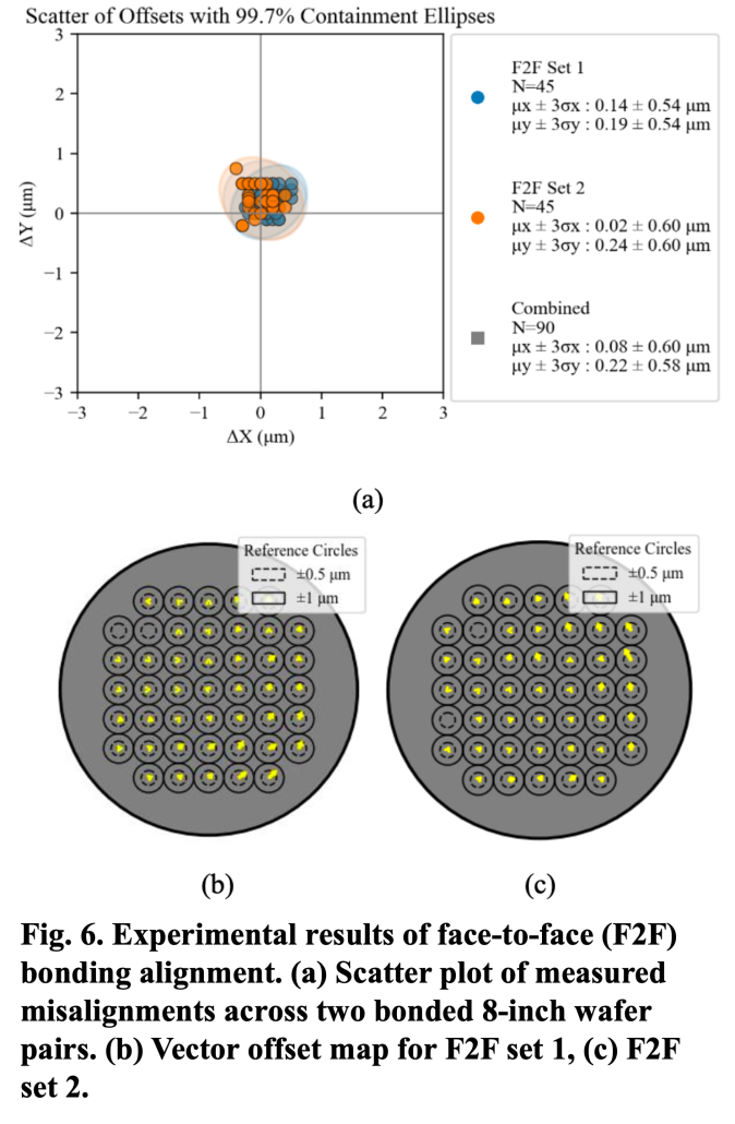
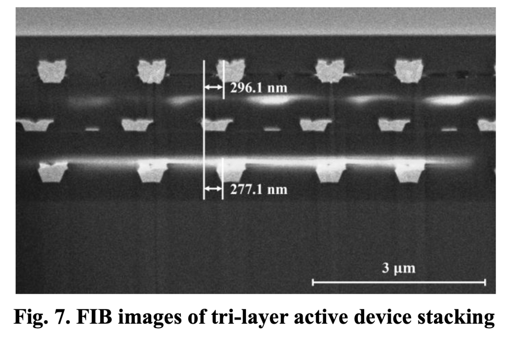
The proposed technology is further demonstrated in 8-inch wafer-to-wafer (W2W) bonding to validate its feasibility for practical 3D integration processes. As shown in Fig. 6, the W2W alignment results achieve global alignment errors of Δx = 0.08 ± 0.60 μm and Δy = 0.22 ± 0.58 μm (Mean ±3σ). The technology is further applied to three-tier active device stacking, as shown in Fig. 7, achieving approximately 300 nm alignment error between adjacent tiers with an interlayer dielectric thickness below 1 μm. These results demonstrate that the integration of Moiré optical alignment marks, Digital Twin, and deep learning enables a non-contact, high-precision, and automated wafer alignment approach, with potential for multi-tier 3D IC integration and high-density heterogeneous integration.
Figure