Through-Glass Via (TGV)
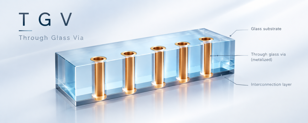
Through-glass via (TGV) technology is one of the key enablers for applying glass substrates in advanced packaging. As high-performance computing, AI accelerators, and high-frequency communication drive growing demands on signal integrity and packaging density, glass substrates—offering low dielectric loss and favorable electrical performance—are attracting increasing attention. Compared with through-silicon vias (TSVs), glass also provides good dimensional stability, a coefficient of thermal expansion (CTE) that can be tailored through material composition, and the cost potential of large-area panel-level processing, making it well suited as a carrier and interposer for 2.5D/3D heterogeneous integration and Co-Packaged Optics (CPO).
However, because glass is brittle, forming high-aspect-ratio vias tends to induce cracking, chipping, and sidewall defects that degrade yield and reliability and limit further scaling of via diameter and density. Establishing a high-precision, low-defect, and stable glass micromachining capability while preserving structural integrity is therefore critical to bringing glass substrates into volume production. This study uses TGVs as the primary test structure and adopts a process route of laser modification combined with selective etching to systematically establish this micromachining capability.
The resulting process is not limited to TGVs; it can be extended to other advanced-packaging microstructures such as optical integration, thermal management, and fiber alignment, offering strong application scalability. Carried out in collaboration with industry partners—combining expertise in glass substrates and process chemistry—the work will continue to optimize via profile and process stability and to evaluate feasibility for volume manufacturing, aiming to accelerate the practical adoption of glass substrates in advanced packaging.
Figure
Related Technology