Monolithic 3DIC
For the monolithic 3DIC, layers of circuits are fabricated sequentially and connected with ultra-dense interlayer via. Accordingly, Monolithic 3D integration can provide efficient connectivity of circuits and decrease power consumption, as well as enhance system performance and reduce chip size. Management of the thermal impact of multi-tiered processes to avoid degradation of transistors and circuits on the underlying layers is the key to realize high performance monolithic 3D integrated circuits. Furthermore, if polycrystalline semiconductor is used, e.g. poly-Si, the yield of Monolithic 3D technology is decreased by the random grain boundaries.
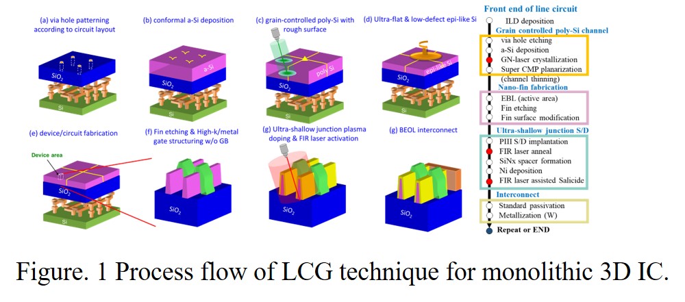
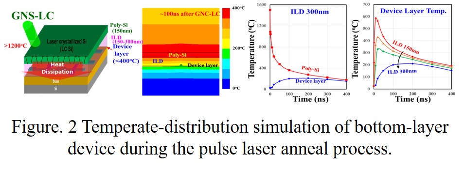
In our team, a BEOL location-controlled grain (LCG) technique has been proposed to fabricate practical monolithic 3D FinFET circuits with controlled thermal budgets by the application of a pulse laser anneal process. The monolithic 3D fabrication with the LCG scheme is introduced as shown in Figure 1. The critical steps are via hole etching into the interlayer-dielectric (ILD) to form “cooling holes”, which can provide selective cooling and crystallization seeding points. Accordingly, a single-grain emerges at the top of the hole during the laser crystallization, achieving regularly patterned array of single-grain Si matrix. In addition, the simulation of computational fluid dynamics tools is performed to evaluate the temperate distribution during pulse laser anneal process, indicating that the temperature of the underlying devices and interconnect is still much less than the BEOL process temperature limit (400 ◦C), as shown in Figure 2.
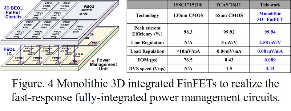
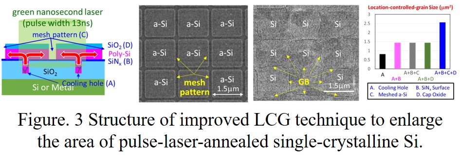
In the following studies by our team, the structure of cooling holes, SiNx interface, meshed a-Si, and capping oxide, is proposed to improve the size of single-crystalline grain to 2.56 μm2, as shown in Figure 3. Based on this improved LCG technique, fast-response fully-integrated power management circuits are fabricated, demonstrating that the response time of 820ns from 1.12V to 0.90V and better theoretical FOM of 0.089ns compared to those of 2D regulators, as shown in Figure 4.
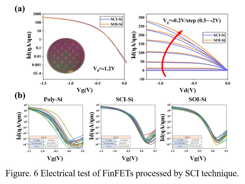
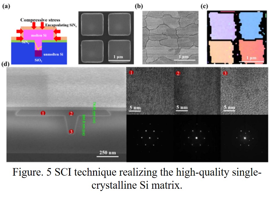
In 2021, our team further proposed the Si single-crystal-islands (SCI) technique. By laser recrystallizing mask-defined a-Si islands encapsulated with conformal SiNx, the quality of single-crystalline Si can be improved, which are validated by Secco Etch, high-resolution electron microscopy (HREM), transmission electron microscopy (TEM), and electron backside scattering (EBSD), as shown in Figure 5. Moreover, about 40 nm FinFETs were successfully fabricated in the SCI Si islands, showing excellent electrical performance and low variability. The results of electrical measurements are compatible with the FinFETs fabricated on commercial silicon-on-insulator (SOI) wafer, as shown in Figure 6.

